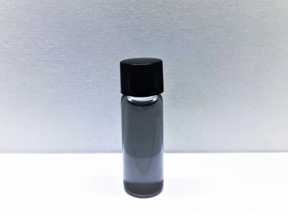
HfSe2溶液是通过将HfSe2薄片悬吊到异丙醇溶液中形成的,但如果需要,可以安排其他类型的溶液。HfSe2晶体前体是在我们的工厂使用最先进的通量区技术开发的。每次生长都需要近三个月的时间来提供完美的不含卤化物的晶体。每个晶体高度结晶,朝向0001方向,容易剥落。我们的研发人员在每个样品中采用特征数据集,以确保结构、光学和电子的一致性。他们被优化以达到完美的工业半导体级材料:1)优秀的化学计量学,2)大型单一域大小,3)单相材料或无定形的内容没有任何混合阶段,4)完美的分层水晶剥落的理想目的与令人印象深刻的马赛克传播0.08度,5)无与伦比的纯净半导体级(6 n), 99.9999%。
溶液类型:由于具有良好的分散性、稳定性和高性能,2Dsemiconductors USA默认提供悬浮在异丙醇中的HfSe2片材。但是,如果您的研究需要其他溶剂,请联系我们更多的细节和产品交付的时间表。
溶液浓度:为了降低运输成本,简化通关手续,我们运送过饱和的2D溶液(根据2D层的类型~100毫克/升)。然而,过饱和的溶液可以稀释成250-500mL的溶液,通过简单而经济的旋转铸造工艺在所需的基质上沉积2D层。
增长方法matters>通量区还是CVT生长法,卤化物污染和层状晶体中的点缺陷是导致其电子迁移率降低、各向异性响应减弱、e-h复合差、低pl发射和低光吸收的主要原因。磁通区技术是一种用于合成真正的半导体级vdW晶体的无卤化物技术。该方法与化学蒸汽输运(CVT)技术的区别在于:CVT是一种生长速度快(~2周)的方法,但晶体质量较差,缺陷浓度可达1E11 ~ 1E12 cm-2。而通量法生长时间较长(~3个月),但结晶速度慢,原子结构完美,无杂质晶体生长,缺陷浓度低至1E9 - 1E10 cm-2。在检查期间,只需声明哪种类型的生长过程是首选的。除非另有说明,2Dsemiconductors磁通区晶体作为默认选择。
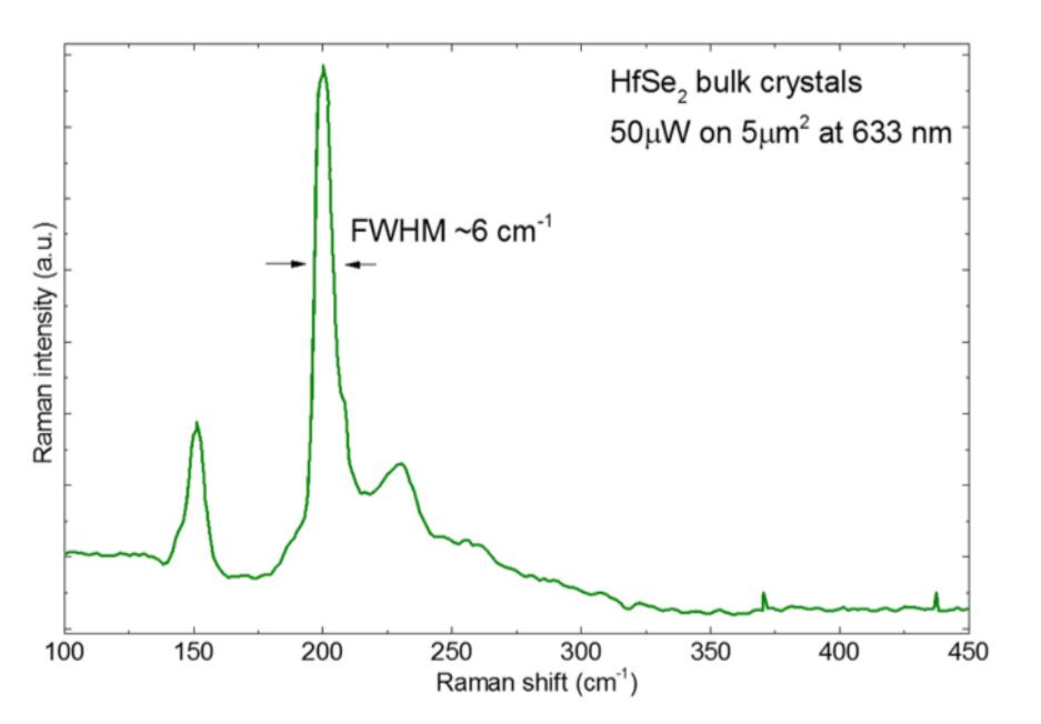
HfSe2 solution has been created by suspending HfSe2 sheets into isopropanol solution but if needed other solution types can be arranged. HfSe2 crystal precursors are developed at our facilities using state-of-art flux zone techniques. Each growth takes close to three months to provide you perfected crystals that does not contain any halides. Each crystal is highly crystalline, oriented in 0001 direction, and easy to exfoliate. Our R&D staff takes characterization dataset in each sample piece to ensure structural, optical, and electronic consistency. They have been optimized to achieve perfect industrial semiconductor grade materials with: 1) excellent stoichiometry, 2) large single domain size, 3) single phase materials without any mixed phases or amorphous content, 4) perfect layered crystal ideal for exfoliation purposes with impressive mosaic spread 0.08 degrees, 5) unmatched purity -semiconductor grade (6N), 99.9999%.
Solution type: By default 2Dsemiconductors USA will provide HfSe2 sheets suspended in isopropanol owing to good dispersion, stability, and high performance. However, if your research requires other solvents, please contact us for more details and schedule for the product delivery.
Solution concentration: To reduce shipping costs, easy customs agreement / border check-in processes, we ship supersaturated 2D solutions (~100 mg/L depending on the type of 2D layers). However, supersaturated solutions can be diluted to produce ~250-500mL of solution to deposit 2D layers onto desired substrates through simple and cost-effective spin-casting process.
Growth method matters> Flux zone or CVT growth method? Contamination of halides and point defects in layered crystals are well known cause for their reduced electronic mobility, reduced anisotropic response, poor e-h recombination, low-PL emission, and lower optical absorption. Flux zone technique is a halide free technique used for synthesizing truly semiconductor grade vdW crystals. This method distinguishes itself from chemical vapor transport (CVT) technique in the following regard: CVT is a quick (~2 weeks) growth method but exhibits poor crystalline quality and the defect concentration reaches to 1E11 to 1E12 cm-2 range. In contrast, flux method takes long (~3 months) growth time, but ensures slow crystallization for perfect atomic structuring, and impurity free crystal growth with defect concentration as low as 1E9 - 1E10 cm-2. During check out just state which type of growth process is preferred. Unless otherwise stated, 2Dsemiconductors ships Flux zone crystals as a default choice.